Wednesday, July 29, 2009

Memory Packaging

First of all, it should be noted that each motherboard supports memory based on the speed of the frontside bus (FSB) and the memory’s form factor.

So, for example, if the motherboard’s FSB is rated at a maximum speed of 533MHz, and you install memory that is rated at 300Mhz, the memory will operate at only 300MHz, thus making the computer operate slower than what it could.

In their specifications, most motherboards list which type(s) of memory they support as well as its maximum speeds.

The memory slots on a motherboard are designed for particular module form factors or styles. In case you run across the older terms, DIP, SIMM, and SIPP are obsolete memory packages.

Terms like double-sided/single-sided memory and dual-bank/single-bank memory are often confused. When speaking of sides, it is correct to refer to the two physical sides of the
module and whether they contain chips.

However, that says nothing of the number of banks the module satisfies. Satisfying two banks, or channels more often, as in the case of the DDR family, can be accomplished with single-sided memory. The most popular form factors for primary memory modules today are these:

  1. DIMM
  2. RIMM
  3. SoDIMM
  4. MicroDIMM
DIMM

One type of memory package is known as a DIMM. As mentioned earlier in this chapter, DIMM stands for Dual Inline Memory Module.

DIMMs are 64-bit memory modules that are used as a package for the SDRAM family: SDRAM, DDR, and DDR2.

The term dual refers to the fact that, unlike their SIMM predecessors, DIMMs differentiate the functionality of the pins on one side of the module from the corresponding pins on the other side.

With 84 pins per side, this makes 168 independent pins on each standard SDRAM module.

The DIMM used for DDR memory has a total of 184 pins and a single keying notch, while the DIMM used for DDR2 has a total of 240 pins, one keying notch, and an aluminum cover for both sides, called a heat spreader, designed like a heat sink to dissipate heat away from the memory chips and prevent overheating.

RIMM

Not an acronym, RIMM is a trademark of Rambus Inc., perhaps a clever play on the acronym DIMM, a competing form factor.

A RIMM is a custom memory module that varies in physical specification based on whether it is a 16-bit or 32-bit module.

The 16-bit modules have 184 pins and two keying notches, while 32-bit modules have 232 pins and only one keying notch, reminiscent of the trend in SDRAM-to-DDR evolution.

The dual-channel architecture can be implemented utilizing two separate 16-bit RIMMs or the newer 32-bit single-module design.

Motherboards with the 16-bit single- or dual-channel implementation provide four RIMM slots that must be filled in pairs, while the 32-bit versions provide two RIMM slots that can be filled one at a time.

A 32-bit RIMM has two 16-bit modules built in and requires only a single motherboard slot, albeit a physically different slot. So you must be sure of the module your motherboard accepts before upgrading.

DIMM

One type of memory package is known as a DIMM.

As mentioned earlier in this chapter, DIMM stands for Dual Inline Memory Module. DIMMs are 64-bit memory modules that are used as a package for the SDRAM family: SDRAM, DDR, and DDR2.

The term dual refers to the fact that, unlike their SIMM predecessors, DIMMs differentiate the functionality of the pins on one side of the module from the corresponding pins on the other side.

With 84 pins per side, this makes 168 independent pins on each standard SDRAM module.

The DIMM used for DDR memory has a total of 184 pins and a single keying notch, while
the DIMM used for DDR2 has a total of 240 pins, one keying notch, and an aluminum cover
for both sides, called a heat spreader, designed like a heat sink to dissipate heat away from the
memory chips and prevent overheating.

RIMM

Not an acronym, RIMM is a trademark of Rambus Inc., perhaps a clever play on the acronym DIMM, a competing form factor.

A RIMM is a custom memory module that varies in physical specification based on whether it is a 16-bit or 32-bit module.

The 16-bit modules have 184 pins and two keying notches, while 32-bit modules have 232 pins and only one keying notch, reminiscent of the trend in SDRAM-to-DDR evolution.

The dual-channel architecture can be implemented utilizing two separate 16-bit RIMMs or the newer 32-bit single-module design.

Motherboards with the 16-bit single- or dual-channel implementation provide four RIMM slots that must be filled in pairs, while the 32-bit versions provide two RIMM slots that can be filled one at a time.

A 32-bit RIMM has two 16-bit modules built in and requires only a single motherboard slot, albeit a physically different slot.

So you must be sure of the module your motherboard accepts before upgrading.

MicroDIMM

The newest, and smallest, RAM form factor is the MicroDIMM.

The MicroDIMM is an extremely small RAM form factor.

In fact, it is over 50 percent smaller than a SoDIMM, only 45.5 millimeters (about 1.75 inches) long and 30 millimeters (about 1.2 inches—a bit bigger than a quarter) wide.

It was designed for the ultralight and portable subnotebook style of computer (like those based on the Transmeta Crusoe processor).

These modules have 144 pins or 172 pins and are similar to a DIMM in that they use a 64-bit data bus.

Often employed in laptop computers.

EXAMPLES OF RAM

DIMM


DRAM

DRAM is dynamic random access memory. (This is what most people are talking about when they mention RAM.)

When you expand the memory in a computer, you are adding DRAM chips.

You use DRAM to expand the memory in the computer because it’s cheaper than any other type of memory.

Dynamic RAM chips are cheaper to manufacture than other types because they are less
complex.

Dynamic refers to the memory chips’ need for a constant update signal (also called a
refresh signal) in order to keep the information that is written there.

If this signal is not received every so often, the information will cease to exist. Currently, there are four popular implementations of DRAM: SDRAM, DDR, DDR2, and RAMBUS.

SDRAM

The original form of DRAM had an asynchronous interface, meaning that it derived its clocking
from the actual inbound signal, paying attention to the electrical aspects of the waveform, such
as pulse width, to set its own clock to synchronize on the fly with the transmitter.

Synchronous DRAM (SDRAM) shares a common clock signal with the transmitter of the data.

The computer’s system bus clock provides the common signal that all SDRAM components use for each step to be performed.

This characteristic ties SDRAM to the speed of the FSB and the processor, eliminating the
need to configure the CPU to wait for the memory to catch up.

Every time the system clock ticks, one bit of data can be transmitted per data pin, limiting the bit rate per pin of SDRAM to the corresponding numerical value of the clock’s frequency.

With today’s processors interfacing with memory using a parallel data-bus width of 8 bytes (hence the term 64-bit processor), a 100MHz clock signal produces 800MBps.

That’s megabytes per second, not megabits. Such memory is referred to as PC100, because throughput is easily computed as eight times the rating.

DDR

Double Data Rate (DDR) SDRAM earns its name by doubling the transfer rate of ordinary SDRAM by double-pumping the data, which means transferring it on both the rising and
falling edges of the clock signal.

This obtains twice the transfer rate at the same FSB clock frequency. It’s the rising clock frequency that generates heating issues with newer components, so keeping the clock the same is an advantage.

The same 100MHz clock gives a DDR SDRAM system the impression of a 200MHz clock in comparison to a single data rate (SDR) SDRAM system.

You can use this new frequency in your computations or simply remember to double your results for SDR calculations, producing DDR results.

For example, with a 100MHz clock, two operations per cycle, and 8 bytes transferred per operation, the data rate is 1600MBps.

Now that throughput is becoming a bit tricker to compute, the industry uses this final figure to name the memory modules instead of the frequency, which was used with SDR.

This makes the result seem many times better, while it’s really only twice as good. In this example, the module is referred to as PC1600.

The chips that go into making PC1600 modules are named after the perceived double-clock frequency: DDR-200.

DDR2

Think of the 2 in DDR2 as yet another multiplier of 2 in the SDRAM technology, using a lower peak voltage to keep power consumption down (1.8V vs. the 2.5V of DDR and others).

Still double-pumping, DDR2, like DDR, uses both sweeps of the clock signal for data transfer.

Internally, DDR2 further splits each clock pulse in two, doubling the number of operations it
can perform per FSB clock cycle.

Through enhancements in the electrical interface and buffers, as well as through adding off-chip drivers, DDR2 nominally produces four times what SDR is capable of producing.

However, DDR2 suffers from enough additional latency over DDR that identical throughput ratings find DDR2 at a disadvantage.

Once frequencies develop for DDR2 that do not exist for DDR, however, DDR2 could become the clear SDRAM leader, although DDR3 is nearing release.

Continuing the preceding example and initially ignoring the latency issue, DDR2 using a 100MHz clock transfers data in four operations per cycle and still 8 bytes per operation, for a total of 3200MBps.

Just like DDR, DDR2 names its chips based on the perceived frequency. In this case, you would be using DDR2-400 chips.

DDR2 carries on the final-result method for naming modules but cannot simply call them PC3200 modules because those already exist in the DDR world. DDR2 calls these modules PC2-3200.

The latency consideration, however, means that DDR’s PC3200 offering is preferable to DDR2’s PC2-3200.

After reading the “RDRAM” section, consult Table 1.2 below , which summarizes how each technology in the “DRAM” section would achieve a transfer rate of 3200MBps, even if only theoretically.

For example, SDR PC400 doesn’t exist.


RDRAM

Rambus DRAM, or Rambus Direct RAM (RDRAM), named for the company that designed
it, is a proprietary synchronous DRAM technology.

RDRAM can be found in fewer new systems today than just a few years ago.

This is because Intel once had a contractual agreement with Rambus to create chipsets for the motherboards of Intel and others that would primarily use RDRAM in exchange for special licensing considerations and royalties from Rambus.

The contract ran from 1996 until 2002.

In 1999, Intel launched the first motherboards with RDRAM support.

Until then, Rambus could be found mainly in gaming consoles and home theater components.

RDRAM did not impact the market as Intel had hoped, and so motherboard manufacturers got around Intel’s obligation by using chipsets from VIA Technologies, leading to the rise of that company.

Although other specifications preceded it, the first motherboard RDRAM model was known as PC800.

As with non-RDRAM specifications that use this naming convention, PC800 specifies that, using a faster 400MHz clock signal and double-pumping like DDR/DDR2, an effective frequency of 800MHz and a transfer rate of 800Mbps per data pin are created.

PC800 uses only a 16-bit (2-byte) bus called a channel, exchanging a 2-byte packet during each read/write cycle, still bringing the overall transfer rate to 1600MBps per channel because of the much higher clock rate. Modern chipsets allow two 16-bit channels to communicate simultaneously for the same read/ write request, creating a 32-bit dual-channel.

Two PC800 modules in a dual-channel configuration produce transfer rates of 3200MBps.

Today, RDRAM modules are also manufactured for 533MHz and 600MHz bus clock frequencies and 32-bit dual-channel architectures.

Termed PC1066 and PC1200, these models produce transfer rates of 2133 and 2400MBps per channel, respectively, making 4266 and 4800MBps per dual-channel.

Rambus has road maps to 1333 and 1600MHz models.

The section “RIMM” in this chapter details the physical details of the modules. Despite RDRAM’s performance advantages, it has some drawbacks that keep it from taking over the market.

Increased latency, heat output, complexity in the manufacturing process, and cost are the primary shortcomings.

PC800 RDRAM had a 45ns latency, compared to only 7.5ns for PC133 SDR SDRAM.

The additional heat that individual RDRAM chips put out led to the requirement for heat sinks on all modules.

High manufacturing costs and high licensing fees led to triple the cost to consumers over SDR, although today there is more parity between the prices.

In 2003, free from its contractual obligations to Rambus, Intel released the i875P chipset. This new chipset provides support for a dual-channel platform using standard PC3200 DDR
modules.

Now, with 16 bytes (128 bits) transferred per read/write request, making a total transfer rate of 6400MBps, RDRAM no longer holds the performance advantage it once did.

SRAM

The S in SRAM stands for static.

Static random access memory doesn’t require a refresh signal
like DRAM does.

The chips are more complex and are thus more expensive.

However, they are faster. DRAM access times come in at 60 nanoseconds (ns) or more; SRAM has access times as fast as 10ns.

SRAM is often used for cache memory.

ROM

ROM stands for read-only memory.

It is called read-only because the original form of this memory could not be written to.

Once information had been written to the ROM, it couldn’t be changed. ROM is normally used to store the computer’s BIOS, because this information normally does not change very often.

The system ROM in the original IBM PC contained the power-on self-test (POST), Basic Input/Output System (BIOS), and cassette BASIC.

Later IBM computers and compatibles include everything but the cassette BASIC.

The system ROM enables the computer to “pull itself up by its bootstraps,” or boot (start the operating system).

Through the years, different forms of ROM were developed that could be altered.

The first generation was the programmable ROM (PROM), which could be written to for the first time in the field, but then no more.

Following the PROM came erasable PROM (EPROM), which was able to be erased using ultraviolet light and subsequently reprogrammed.

These days, our flash memory is a form of electrically erasable PROM (EEPROM), which does not require UV light, but rather a slightly higher than normal electrical pulse, to erase its contents.

CMOS

CMOS is a special kind of memory that holds the BIOS configuration settings.

CMOS memory is powered by a small battery, so the settings are retained when the computer is shut off.

The BIOS starts with its own default information and then reads information from the CMOS, such as which hard drive types are configured for this computer to use, which drive(s) it should search for boot sectors, and so on.

Any conflicting information read from the CMOS overrides the default information from the BIOS.

CMOS memory is usually not upgradable in terms of its capacity and is very often integrated into the modern BIOS chip.

Identifying Purposes and Characteristics of Memory

“More memory, more memory, I don’t have enough memory!” Today, memory is one of the most popular, easy, and inexpensive ways to upgrade a computer.

As the computer’s CPU works, it stores information in the computer’s memory.

The rule of thumb is the more memory a computer has, the faster it will operate.

To identify memory within a computer, look for several thin rows of small circuit boards sitting vertically, packed tightly together near the processor.

Location of memory within a system
Parity


Parity checking is a rudimentary error-checking scheme that lines up the chips in a column and divides them into an equal number of bits, numbered starting at 0.

All the number n bits, one from each chip, form a numerical set. If even parity is used, for example, the number of bits in the set is counted up, and if the total comes out even, then the parity bit is set to 0, because the count is already even. If it comes out odd, then the parity bit is set to 1 to even up the count.

You can see that this is effective only for determining if there was a blatant error in the set of bits, but there is no indication as to where the error is and how to fix it. This is error checking, not error correction.

Finding an error can lock up the entire system and display a memory parity error. Enough of these errors and you need to replace the memory.

If that doesn’t fix the problem, good luck. In the early days of personal computing, almost all memory was parity-based. Compaq was one of the first manufacturers to employ non-parity RAM in their mainstream systems.

As quality has increased over the years, parity checking in the RAM subsystem has become rarer.

If parity checking is not supported, there will generally be fewer chips per module, usually one less per column of RAM.

The next step in the evolution of memory error detection is known as Error Checking and
Correcting (ECC).

If memory supports ECC, check bits are generated and stored with the data. An algorithm is performed on the data and its check bits whenever the memory is accessed. If the result of the algorithm is all zeros, then the data is deemed valid and processing
continues.

ECC can detect single- and double-bit errors and actually correct single-bit errors.

In the following sections, we’ll outline the four major types of computer memory—DRAM, SRAM, ROM, and CMOS—as well as memory packaging.

Identifying Purposes and Characteristics of Memory


Identifying Purposes and Characteristics of Processors


The role of the CPU, or central processing unit, is to control and direct all the activities of the computer using both external and internal buses.

It is a processor chip consisting of an array of millions of transistors.

Older CPUs are generally square, with contacts arranged in a Pin Grid Array (PGA).

Prior to 1981, chips were found in a rectangle with two rows of 20 pins known as a Dual Inline Package (DIP).

There are still integrated circuits that use the DIP form factor.

However, the DIP form factor is no longer used for PC CPUs.

Most CPUs use either the PGA or the Single Edge Contact Cartridge (SECC) form factor.

SECC is essentially a PGA-type socket on a special expansion card.

As processor technology grows and motherboard real estate stays the same, more must
be done with the same amount of space.

To this end, the Staggered PGA (SPGA) layout was developed.

An SPGA package arranges the pins in what appears to be a checkerboard pattern, but if you angle the chip diagonally, you’ll notice straight rows, closer together than the rightangle rows and columns of a PGA.

This feature allows a higher pin count per area.

You can easily identify which component inside the computer is the CPU because it is a large square lying flat on the motherboard with a very large heat sink and fan.

Or if the CPU is installed in a Slot 1 motherboard, it is a large 1⁄2-inch-thick expansion card with a large heat sink and fan integrated into the package.

It is located away from the expansion cards.

Notice how prominent the CPU is.


The location of a CPU inside a typical computer

Hyperthreading

This term refers to Intel’s Hyper-Threading Technology (HTT).

HTT is aform of simultaneous multithreading (SMT).

SMT takes advantage of a modern CPU’s superscalar architecture.

Superscalar processors are able to have multiple instructions operating on separate data in parallel.

HTT-capable processors appear to the operating system to be two processors.

As a result, the operating system can schedule two processes at the same time, as in the case of symmetric multiprocessing (SMP), where two or more processors use the same system resources.

In fact, the operating system must support SMP in order to take advantage of HTT.

If the current process stalls because of missing data caused by, say, cache or branch prediction issues, the execution resources of the processor can be reallocated for a different process that is ready to go, reducing processor downtime.

Multicore

A processor that exhibits a multicore architecture has two completely separate processors
in the same package.

Whether there are multiple dies in the same package or the singledie contains the equivalent circuitry of multiple processors, the operating system can treat the single processor as if it were two separate processors.

As with HTT, the operating system must support SMP.

In addition, SMP is not an enhancement if the applications run on the SMP system are not written for parallel processing.

Dual-core processors are a common specific case for the multi-core technology.

Throttling

CPU throttling, or clamping, is the process of controlling how much CPU time is spent on an application. By controlling how individual applications use the CPU, all applications are treated more fairly.

The concept of application fairness becomes a particular issue in server environments, where each application could represent the efforts of a different user.

Thus, fairness to applications becomes fairness to users, the real customers.

Clients of today’s terminal servers benefit from CPU throttling.


Microcode

Microcode is the set of instructions (known as an instruction set) that make up the various microprograms that the processor executes while carrying out its various duties.

The Multimedia Extensions (MMX) microcode is a specialized example of a separate microprogram that carries out a particular set of functions.

Microcode is at a much lower level than the code that makes up application programs.

Each instruction in an application will end up being represented by many microinstructions, on average.

The MMX instruction set is incorporated into most modern CPUs from Intel and others. MMX came about as a way to take much of the multimedia processing off the CPU’s hands, leaving the processor to other tasks.

Think of it as sort of a coprocessor for multimedia, much like the floating-point unit (FPU) is
a math coprocessor.

Overclocking

Overclocking your CPU offers increased performance, on par with a processor designed to operate at the overclocked speed.

However, unlike with the processor designedto run that fast, you must make special arrangements to ensure that an overclocked CPU does not destroy itself from the increased heat levels.

An advanced cooling mechanism, such as liquid cooling, might be necessary to avoid losing the processor and other components.

Cache

Cache is a very fast chip memory that is used to hold data and instructions that are most likely to be requested next by the CPU.

The cache located on the CPU is known as L1 cache and is generally smaller in comparison to L2 cache, which is located on the motherboard.

When the CPU requires outside information, it believes it requests that information from RAM.

The cache controller, however, intercepts the request and consults its tag RAM to discover if the requested information is already cached, either at L1 or L2.

If not, a cache miss is recorded and the information is brought back from the much slower RAM, but this new information sticks to the L1 and L2 cache on its way to the CPU from RAM.

Voltage Regulator Module

The voltage regulator module (VRM) is the circuitry that sends a standard voltage level to the portion of the processor that is able to send a signal back to the VRM concerning the voltage level the CPU needs.

After receiving the signal, the VRM truly regulates the voltage to steadily provide the requested voltage.

Speed

The speed of the processor is generally described in clock frequency (MHz or GHz).

There can be a discrepancy between the advertised frequency and the frequency the CPU uses
to latch data and instructions through the pipeline.

This disagreement between the numbers comes from the fact that the CPU is capable of splitting the clock signal it receives from the oscillator into multiple regular signals for its own use.

32- and 64-Bit System Bus

The set of data lines between the CPU and the primary memory of the system can be 32 or 64 bits wide, among other widths.

The wider the bus, the more data that can be processed per unit of time, and hence the more work that can be performed.

Internal registers in the CPU might be only 32 bits wide, but with a 64-bit system bus, two separate pipelines can receive information simultaneously.

Firmware

Firmware is the name given to any software that is encoded into a read-only memory (ROM) chip and can be run without extra instructions from the operating system.

Most computers use firmware in some limited sense.

The best example of firmware is a computer’s CMOS setup program, which is used to set the options for the computer’s BIOS (time/date and boot options, for example).

Also, some expansion cards, such as Small Computer System Interface (SCSI) cards, use their own firmware utilities for setting up peripherals.

Jumpers and DIP Switches

The last components of the motherboard we will discuss in this section are jumpers and DIP
switches.

These two devices are used to configure various hardware options on the motherboard.
For example, some processors use different voltages (1.5, 3.3, or 5 volts).

You must set the motherboard to provide the correct voltage for the processor it is using.

You do so by changing a setting on the motherboard with either a jumper or a DIP switch. Motherboards often have either several jumpers or one bank of DIP switches.

Individual jumpers are often labeled with the moniker JPx (where x is the number of the jumper).

CMOS Battery

Your PC has to keep certain settings when it’s turned off and its power cord is unplugged.
These settings include the following:
  1. Date
  2. Time
  3. Hard drive configuration
  4. Memory
Your PC keeps these settings in a special memory chip called the Complimentary Metal Oxide Semiconductor (CMOS) chip.

Actually, CMOS (usually pronounced see-moss) is a type of memory chip; it is the parameter memory for the BIOS. But that doesn’t translate into an easy-to-say acronym.

So because it’s the most important CMOS chip in the computer, it has come to be called the CMOS.

To keep its settings, the memory must have power constantly. When you shut off a computer,
anything that is left in main memory is lost forever.

To prevent CMOS from losing its information (and it’s rather important that it doesn’t), motherboard manufacturers include a small battery called the CMOS battery to power the CMOS memory.

The batteries come in different shapes and sizes, but they all perform the same function. Most CMOS batteries look like either large watch batteries or small, cylindrical batteries.

BIOS Chip

Aside from the processor, the most important chip on the motherboard is the Basic Input/Output System (BIOS) chip.

This special memory chip contains the BIOS software that tells the processor how to interact with the rest of the hardware in the computer.

The BIOS chip is easily identified: If you have a non-clone computer (Compaq, IBM, HP, and so on), this chip has on it the name of the manufacturer and usually the word BIOS.

For example, the BIOS chip for a Compaq has something like Compaq BIOS printed on it. For clones, the chip usually has a sticker or printing on it from one of the major BIOS manufacturers (AMI, Phoenix/Award, Winbond, and so on).

Motherboard Attachment

There are two ways of connecting these ports to the motherboard (assuming the circuitry for
providing these functions is integrated into the motherboard).

The first, called a header connection, allows you to mount the ports into the computer’s case, usually on the backplane, with a special cable connected to a header, or male connector that terminates the motherboard’s traces for that function.

The second method of connecting a peripheral port is known as the direct-solder method.

With this method, the individual ports are soldered directly to the motherboard.

This method is used mostly in integrated motherboards in non-clone machines.

Notice that there is no cable between the port and the motherboard and that the port is part of the motherboard.

As discussed earlier, these onboard ports can be disabled in the BIOS setup if necessary.


Connecting a port to the header on a motherboard


Peripheral ports directly soldered to a motherboard

Peripheral Ports and Connectors

In order for a computer to be useful and have the most functionality, there must be a way to get the data into and out of it.

Many different ports are available for this purpose.

Briefly, the seven most common types of ports you will see on a computer are serial, parallel,
Universal Serial Bus (USB), video, Ethernet, sound in/out, and game ports.

  1. DC power in
  2. Analog modem RJ-11
  3. Ethernet NIC RJ-45
  4. S-video out
  5. DVI-D out
  6. SVGA out
  7. Parallel (on top)
  8. Standard serial
  9. Mouse (on top)
  10. Keyboard
  11. S/PDIF (out)
  12. USB
Peripheral Ports and Connectors


Game Port

Keyboard Connectors

The most important input device for a PC is the keyboard. All PC motherboards contain a connector that allows a keyboard to be connected directly to the motherboard through the case.

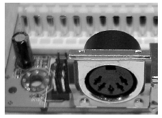
There are two main types of keyboard connectors. Once, these were the AT and PS/2 connectors. Today, the PS/2-style connector remains popular, but it is quickly being replaced by USB-attached keyboards.

The all-but-extinct original AT connector is round, about 1⁄2 inch in diameter, in a 5-pin DIN configuration.

The PS/2 connectoris a smaller 6-pin mini-DIN connector.

Most new PCs you can purchase today contain a PS/2 keyboard connector as well as a PS/2 mouse connector right above it on the motherboard.

AT keyboard connector


PS2 keyboard connector

Onboard Floppy and Hard Disk Connectors

Almost every computer made today uses some type of disk drive to store data and programs until they are needed.

Most drives need a connection to the motherboard so the computer can “talk” to the disk drive.

These connections are known as drive interfaces, and there are two main types: floppy drive interfaces and hard disk interfaces.

Floppy disk interfaces allow floppy disk drives (FDDs) to be connected to the motherboard and, similarly, hard disk interfaces do the same for hard disks.

When you see them on the motherboard, these interfaces are said to be onboard, as opposed to being on an expansion card (off-board). The interfaces consist of circuitry and a port.

Most motherboards produced today include both the floppy disk and hard disk interfaces on the motherboard.

Today, the headers you will find on most motherboards are for Enhanced IDE (EIDE/PATA) or Serial ATA (SATA).

Advanced Technology Attachment (ATA) is the standard term for what is more commonly referred to as Integrated Drive Electronics (IDE).

The AT component of the name was borrowed from the IBM PC/AT, which was the standard of the day.

However, because ATA is not the only technology that integrates the drive controller circuitry into the drive assembly (ESDI, for example, was another), IDE is somewhat of a misnomer and not the best term when referring only to ATA drives.

Nevertheless, the original ATA standard was referred to as IDE and had an upper limit of
528MB per logical drive.

An enhanced version, Enhanced IDE (EIDE), was developed to circumvent the obstacles to accessing more drive space per volume, increasing the limit to 8GB.

Since then, the limit has been increased to 144PB through various enhancements. A petabyte
(PB) is the number of bytes represented by 2 raised to the 50th power.

If your motherboard has PATA headers, they will normally be black or some other neutral color if they follow the classic ATA 40-wire standard.

If your PATA headers are blue, these represent PATA interfaces that employ the Ultra DMA (UDMA) technology that increases transfer rates by reducing crosstalk in the parallel signal by alternating another 40 wires that act as grounds among the other wires.

The connectors and headers are still 40 pins, however.

The color coding alerts you to the enhanced performance, which is downward compatible with the 40-wire technology.

The original 40-pin ATA header transfers data between the drive and motherboard multiple bits in parallel, hence the name Parallel ATA (PATA).

SATA, in comparison, which came out later and prompted the retroactive PATA moniker, transfers data in serial, allowing a higher data throughput because there is no need for more advanced parallel synchronization of data signals.

The SATA headers are vastly different from the PATA headers.

Many motherboards, especially higher-end boards like those found in servers, also include the more complex SCSI circuitry built in so that SCSI-attached drives can connect directly to the system board without an external adapter.

a SATA connector


Power Connectors

In addition to these sockets and slots on the motherboard, a special connector allows the motherboard to be connected to the power supply to receive power.

This connector is where the ATX power connector (mentioned later in this chapter in the
section “Identifying Purposes and Characteristics of Power Supplies”) plugs in.


An ATX power connector on a motherboard

Tuesday, July 28, 2009

Central Processing Unit (CPU) and Processor Socket or Slot

The “brain” of any computer is the central processing unit (CPU).

This component does all the calculations and performs 90 percent of all the functions of a computer.

Typically, in today’s computers, the processor is the easiest component to identify on the motherboard.

It is usually the component that has either a fan or a heat sink (usually both) attached to it .

These devices are used to draw away the heat a processor generates. This is done because heat is the enemy of microelectronics.

Theoretically, a Pentium (or higher) processor generates enough heat that without the heat sink it would self-destruct in a matter of hours.

Sockets and slots on the motherboard are as plentiful and varied as processors. Sockets are basically flat and have several rows of holes arranged in a square.

The processor slot is another method of connecting a processor to a motherboard, but one into
which an Intel Pentium II or Pentium III–class processor on a special expansion card can be
inserted .

Newer, more complex processors, such as the Intel Itanium, use a package known as a pin array cartridge (PAC).

The socket that receives a PAC works on the very low insertion force (VLIF) principle.


picture of processor fan and heat sink


example of CPU socket


example of slot 1 connector slot


Memory Slots and External Cache

Memory or random access memory (RAM) slots are the next most prolific slots on a motherboard, and they contain the modules that hold memory chips that make up primary memory, the memory used to store currently used data and instructions for the CPU.

Many and varied types of memory are available for PCs today

For the most part, PCs today use memory chips arranged on a small circuit board. Certain
of these circuit boards are called Dual Inline Memory Modules (DIMMs).

Today’s DIMMs differ in the number of conductors, or pins, that the particular physical specification uses.

Some common examples include 168-, 184-, and 240-pin configurations. In addition, laptop
memory comes in smaller form factors known as Small Outline DIMMs (SoDIMMs) and MicroDIMMs.

Memory slots are easy to identify on a motherboard. DIMM slots are usually black and
placed very close together.

The number of memory slots varies from motherboard to motherboard, but the appearance of the different slots is similar.

Metal pins in the bottom make contact with the soldered tabs on each memory module.

Small metal or plastic tabs on each side of the slot keep the memory module securely in its slot.
Sometimes primary memory gets a bit overwhelmed with the requests coming from the processor.

To get its bearings, the RAM must obtain the information the CPU wants immediately, but
RAM is not as fast as the CPU, and the CPU must wait.

The result is that the entire system slows down noticeably, on average. One solution for this is to use the hard drive as RAM.

This space on the hard drive is known as virtual RAM (VRAM). VRAM is a contiguous, optimized space that can deliver information to RAM faster than if it came from the general storage pool of the drive.


picture of different memory modules


There is something that can be done on the CPU side of RAM to speed things up a bit as well.

That something is adding cache memory. Cache memory is a very fast form of memory forged
from static RAM, which is discussed in detail in the “Identifying Purposes and Characteristics
of Memory” section of this chapter.

Cache improves system performance by predicting what the CPU will ask for next and prefetching this information before being asked.

This paradigm allows the cache to be smaller in size than the RAM itself. Only the most recently used data and code or that which is expected to be used next is stored in cache. Cache on the motherboard is known as external cache because it is external to the processor.

Also called Level 2 (L2) cache, this is as opposed to the Level 1 (L1) cache built into the processor.

Expansion Slots

The most visible parts of any motherboard are the expansion slots. These look like small plastic slots, usually from 3 to 11 inches long and approximately 1⁄2 inch wide.

As their name suggests, these slots are used to install various devices in the computer to expand its capabilities.

Some expansion devices that might be installed in these slots include video, network, sound, and disk interface cards.

If you look at the motherboard in your computer, you will more than likely see one of the main types of expansion slots used in computers today:
  1. ISA
  2. PCI
  3. AGP
  4. PCIe
  5. AMR
  6. CNR
Each type differs in appearance and function. In this section, we will cover how to visually identify the different expansion slots on the motherboard.

ISA Expansion Slots

If you have a computer made before 1997, chances are the motherboard has a few Industry Standard Architecture (ISA) expansion slots.

They’re easily recognizable because they are usually black and have two parts: one shorter and one longer.

Computers made after 1997 generally include a few ISA slots for backward compatibility with old expansion cards (although most computers are phasing them out in favor of PCI).


picture of ISA slots


PCI Expansion Slots


Most computers made today contain primarily Peripheral Component Interconnect (PCI) slots.

They are easily recognizable because they are short (around 3 inches long) and usually white.

PCI slots can usually be found in any computer that has a Pentium-class processor or higher.


Picture of PCI expansion slots


AGP Expansion Slots


Accelerated Graphics Port (AGP) slots are very popular for video card use. In the past, if
you wanted to use a high-speed, accelerated 3D graphics video card, you had to install the
card into an existing PCI or ISA slot.

AGP slots were designed to be a direct connection between the video circuitry and the PC’s memory.

They are also easily recognizable because they are usually brown, are located right next to the PCI slots on the motherboard, and are shorter than the PCI slots.


AGP slot


PCIe Expansion Slots

The newest expansion slot architecture that is being used by motherboards is PCI Express
(PCIe). It was designed to be a replacement for AGP and PCI.

It has the capability of being faster than AGP while maintaining the flexibility of PCI. And motherboards with PCIe will have regular PCI slots for backward compatibility with PCI.

There are seven different speed levels for PCIe, and they are designated 1X, 2X, 4X, 8X, 12X, 16X, and 32X.

These designations roughly correspond to similarly designated AGP speeds. The slots for PCIe are a bit harder to identify than other expansion slot types because the slot size corresponds to its speed.

For example, the 1X slot is extremely short (less than an inch). The slots get longer in proportion to the speed; the longer the slot, the higher the speed.

The reason for this stems from the PCIe concept of lanes, which are the multiplied units of communication between any two PCIe components and are directly related to physical wiring
on the bus.

Because all PCIe communications are made up of unidirectional coupling between devices, each PCIe card negotiates for the best mutually supported number of lanes with each
communications partner.


PCI Express slots (from top to bottom: x4 , x16, x1 and x16),
compared to a traditional 32-bit PCI slot (bottom),
as seen on DFI's LanParty nF4 SLI-DR.


AMR Expansion Slots


As is always the case, Intel and other manufacturers are constantly looking for ways to improve the production process.

One lengthy process that would often slow down the production of motherboards with integrated analog I/O functions was FCC certification.

The manufacturers developed a way of separating the analog circuitry, for example, modem and
analog audio, onto its own card.

This allowed the analog circuitry to be separately certified (it was its own expansion card), thus reducing time for FCC certification.

This slot and riser card technology was known as the Audio Modem Riser, or AMR. AMR’s 46-pin slots were once fairly common on many Intel motherboards, but technologies including CNR and Advanced Communications Riser (ACR) are edging out AMR.

In addition and despite FCC concerns, integrated components still appear to be enjoying the most success comparatively.


picture of AMR slot


CNR Expansion Slots


The Communications and Networking Riser (CNR) slots that can be found on some Intel
motherboards are a replacement for Intel’s AMR slots.

Essentially, these 60-pin slots allow a motherboard manufacturer to implement a motherboard chipset with certain integrated features.

Then, if the built-in features of that chipset need to be enhanced (by adding Dolby Digital Surround to a standard sound chipset, for example), a CNR riser card could be added to enhance the onboard capabilities.

Additional advantages of CNR over AMR include networking support, Plug and Play compatibility, support for hardware acceleration (as opposed to CPU control only), and no need to lose a competing PCI slot unless the CNR slot is in use.

arrow show the CNR slot

Chipsets


A typical motherboard chipset
(click image for bigger image)

A chipset is a collection of chips or circuits that perform interface and peripheral functions for the
processor.

This collection of chips is usually the circuitry that provides interfaces for memory, expansion cards, and onboard peripherals and generally dictates how a motherboard will talk to the installed peripherals.

Chipsets are usually given a name and model number by the original manufacturer. For example, if you see that motherboard has a VIA KT7 chipset, you would know that the circuitry for controlling peripherals was designed by VIA and was given the designation KT7.

Typically, that would also mean that you would know that a particular chipset has a certain set of features (for example, onboard video of a certain type/brand, onboard audio of a particular
type, and so on).

Chipsets can be made up of one or several integrated circuit chips. Intel-based motherboards typically use two chips, whereas the SiS chipsets typically use one. To know for sure, you must check the manufacturer’s documentation.

The functions of chipsets can be divided into two major functional groups, called Northbridge and Southbridge.

Northbridge

The Northbridge subset of a motherboard’s chipset is the set of circuitry or chips that performs
one very important function: management of high-speed peripheral communications.

The Northbridge subset is responsible primarily for communications with integrated video using
AGP and PCIe, for instance, and processor-to-memory communications.

Therefore, it can be said that much of the true performance of a PC relies on the performance of the Northbridge chipset and the communications between it and the peripherals it controls.

The communications between the CPU and memory occur over what is known as the frontside bus (FSB), which is just a set of signal pathways between the CPU and main memory. The backside bus, on the other hand, is a set of signal pathways between the CPU and Level 2 cache
memory (if present).

The Northbridge chipsets also manage the communications between the Southbridge chipset (discussed next) and the rest of the computer.

Finally, if a motherboard has onboard video circuitry (especially if it needs direct access to main memory), that circuitry will be found within the Northbridge chipset.

Southbridge

The Southbridge chipset, as mentioned earlier, is responsible for providing support to the myriad onboard peripherals (PS/2, Parallel, IDE, and so on), managing their communications with the rest of the computer and the resources given to them.

Most motherboards today have integrated PS/2, USB, Parallel, and Serial. Some of the optional features handled by the Southbridge include LAN, audio, infrared, and FireWire
(IEEE 1394).

When first integrated, the quality of onboard audio was marginal at best, but the latest offerings (such as the AC97 audio chipset) rival Creative Labs in sound quality and number of features (even including Dolby Digital Theater Surround technology).

The Southbridge chipset is also responsible for managing communications with the other expansion buses, such as PCI, USB, and legacy buses.

System Board Components


click pic for bigger image
  1. Chipsets
  2. Expansion slots
  3. Memory slots and external cache
  4. CPU and processor slots or sockets
  5. Power connectors
  6. Onboard disk drive connectors
  7. Keyboard connectors
  8. Peripheral port and connectors
  9. BIOS chip
  10. CMOS battery
  11. Jumpers and DIP switches
  12. Firmware

Mainboard Picture


click the picture to make it bigger and clear


ASUS P5K3 Premium Black Pearl Edition (Intel P35)


System Board Form Factors

System boards are also classified by their form factor (design):

ATX, micro ATX, BTX, or NLX (and variants of these). Exercise care and vigilance when acquiring a motherboard and case separately.

Some cases are less flexible than others and might not accommodate the motherboard you choose.

Advanced Technology Extended (ATX)

The ATX motherboard has the processor and memory slots at right angles to the expansion cards.

This arrangement puts the processor and memory in line with the fan output of the power supply, allowing the processor to run cooler.

And because those components are not in line with the expansion cards, you can install full-length expansion cards in an ATX motherboard machine.

ATX (and its derivatives) are the primary motherboards sold today.

Micro ATX

One form factor that is designed to work in standard ATX cases, as well as its own smaller cases,
is known as micro ATX (also referred to as μATX).

Micro ATX follows the same principle of component placement for enhanced cooling over pre-ATX designs but with a smaller footprint. With this smaller form come trade-offs.

For the compact use of space, you must give up quantity:

quantity of memory modules, quantity of motherboard headers, quantity of expansion slots,
quantity of integrated components, even quantity of micro ATX chassis bays, although the same
small-scale motherboard can fit into much larger cases, if your original peripherals are still a
requirement.

Be aware, however, that micro ATX systems tend to be designed with power supplies of
lower wattage, in order to help keep down power consumption and heat production, which
is generally acceptable with the standard micro ATX suite of components.

As more off-board USB ports are added and larger cases are used with additional in-case peripherals, larger power supplies might be required.

New Low-profile Extended (NLX)

An alternative motherboard form factor, known as New Low-profile Extended (NLX), is used in
some low-profile case types.

NLX continues the trend of the technology it succeeded, Low Profile Extended (LPX), placing the expansion slots (ISA, PCI, and so on) sideways on a special riser card to use the reduced vertical space optimally.

Adapter cards, or daughter boards, that normally plug into expansion slots vertically in ATX motherboards, for example, plug in parallel to the motherboard, so their most demanding dimension does not affect case height.

LPX, a technology that lacked formal standardization and whose riser card interfaces varied from vendor to vendor, enjoyed great success in the 1990s until the advent of the
Pentium II processor and the Accelerated Graphics Port (AGP).

These two technologies placed a spotlight on how inadequate LPX was at cooling and accommodating high pin counts.

NLX, an official standard from Intel, IBM, and DEC, was designed to fix the variability and other
shortcomings of LPX, but NLX never quite caught on the way LPX did.

Newer technologies, such as micro ATX, and proprietary solutions have been more successful and have taken even more market share from NLX.

Balanced Technology Extended (BTX)

In 2003, Intel announced its design for a new motherboard, slated to hit the market mid- to
late-2004. When that time came, the new BTX motherboard was met with mixed emotions.

(Postpone accusations of acronym reverse-engineering until “CTX” is announced as the name
of the next generation.)

Intel and its consumers realized that the price for faster components
that produced more heat would be a retooling of the now-classic (since mid-1990s) ATX
design.

The motherboard manufacturers saw research and development expense and potential
profit loss simply to accommodate the next generation of hotter-running processors, processors
manufactured by the same designers of the BTX technology.

It was this resistance that caused the BTX form factor to gain very little ground over the next couple of years. Nevertheless, with the early support of Gateway, Inc., and later buy-in of Dell, Inc., the BTX design dug in and charted a path for future success.

Marketing aside, the BTX technology is well thought out and serves the purpose for which
it was intended.

By lining up all heat-producing components between air intake vents and the power supply’s exhaust fan, Intel found that the CPU and other components could be cooled
properly by passive heat sinks.

Fewer fans and a more efficient airflow path create a quieter configuration
overall.

While the BTX design benefits any modern onboard implementation, Intel’s
recommitment to lower-power CPUs has at once lessened the need to rush to more expensive
BTX systems and given the market a bit more time to assimilate this newer technology.

There are other motherboard designs, but these are the most popular and also the ones that are covered on the exam.

Some manufacturers (such as
Compaq and IBM) design and manufacture their own motherboards, which don’t conform to the standards. This style of motherboard is known as a proprietary design motherboard.

Identifying Components of Motherboards

Types of System Boards

There are two major types of system boards: integrated and nonintegrated:

Nonintegrated System Board

Each major assembly is installed in the computer as an expansion
card.
The major assemblies we’re talking about are items like the video circuitry, disk controllers,and accessories.

Nonintegrated system boards can be easily identified because each expansion slot is usually occupied by one of these components.

It is difficult to find nonintegrated motherboards these days.

Many of what would normally be called nonintegrated system boards now incorporate the most commonly used circuitry (such as IDE and floppy controllers, serial controllers, and sound cards) onto the motherboard itself.

In the early 1990s, these components had to be installed externally to the motherboard.

Integrated System Board

Most of the components that would otherwise be installed as expansion cards are integrated into the motherboard circuitry.

Integrated system boards were designed for simplicity. Of course, there’s a drawback to this simplicity:

When one component breaks, you can’t just replace the component that’s broken; the whole motherboard must be replaced.

Although these boards are cheaper to produce, they are more expensive to repair.

With integrated system boards, there is a way around having to replace the whole motherboard
when a single component breaks.

On some motherboards, you can disable the malfunctioning
onboard component (for example, the sound circuitry) and simply add an expansion card to
replace its functions.

Identifying Personal Computer Components

In this chapter, you will learn how to identify personal computer components, including
the following:

  1. Motherboards
  2. Processors
  3. Memory
  4. Storage devices
  5. Power supplies
  6. Display devices
  7. Input devices
  8. Adapter cards
  9. Ports and cables
  10. Cooling systems

Information About DDC 3332 Computer Installation and Maintenance

All the note and assignment will be given through this blog, so please make sure you surf it at least once a week..

Any questions, you can ask me by this blog, by mail or meeting me at my room..